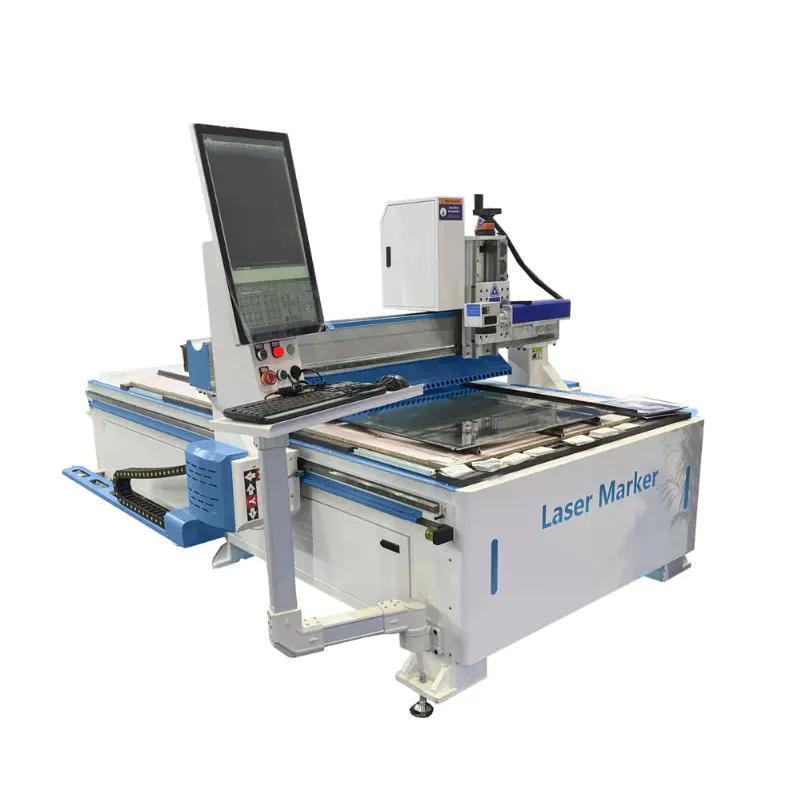


Fiber Laser Welding Machine 4 in 1 Handheld Laser Welding Machine 2000W Handheld Welding Machine for Metal
Enclosed Type
Lithography machine can be used in the making of microfluidic he exactly and what is the difference between etching machine
by:Transon
2021-01-08
In recent years, lithography and etching machine has been the hottest topic.
Lithography, as it were, is the soul of chip manufacturing, and etching machine is the soul of the chips.
To create high-end chip, these two things must be first-class.
the two machines the simplest explanation is that the projection lithography will diagram and in the covered with light to resist on the silicon wafer, and the etching machine will spare circuit diagram on just draw the silicon wafers. A circuit diagram that doesn't seem to be difficult. Yes, but the image is a metaphor. Each chip circuit structure of expanded the number of times, and is more comprehensive than the whole Beijing. This is the difficulty of lithography and sculpture.
lithography process, including on the surface of the silicon wafers that have been coated with a layer of light to resist, Substance similar to the gel, the corrosion may be limited by light) And then the light passing through ( Process is difficult, ultraviolet light & lt; Deep ultraviolet & lt; Extreme ultraviolet light) Circular silicon surface radiation through the mask ( Similar to the projection) 。 Because photoresist are covered, so were part of irradiation was recorded and is not lighting part of the left. This part is the circuit structure.
there are two types of etching, one is the dry etching, the other is the wet etching ( The mainstream) 。 As the name implies, wet etching is added in the process of water. The lithography wafer with a specific chemical reaction solution. The rest is the structure of the circuit. Dry carving unrealized commercial batch production. Principle is the use of plasma instead of chemical solutions to eliminate unnecessary circular silicon components.
at present, the etching machine in China and the development of lithography is a pity, but also in a very local situation: China's microelectronics mass production 7 nm carving machine has direct access to the world's most popular column. As the 90 nanometer lithography in Shanghai microelectronics and the shadow of wuxi speed 200 nm lithography, are far from achieving the world's most advanced 7 nm process. In the two paths, we will continue to make persistent efforts.
Custom message
Related Products